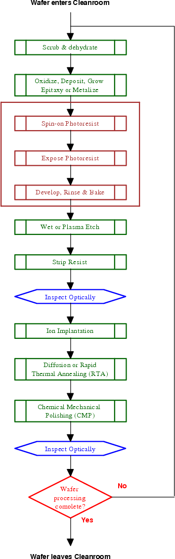
Wafer Fabrication Process Flow
To produce these wafers two sili- con wafers are bonded together by using silicon. The first part of this is called photolithography writing on stone with light.
Semiconductor Wafer Fabrication Process Flow Download Scientific Diagram
Silicon wafers are available in a variety of sizes ranging from 254 mm 1 inch to 300 mm 118 inches.
. It undergoes many microfabrication processes such as doping ion. Each step adds a new layer to the wafer or modifies the existing one. Silicon wafers have been used abundantly in microelectronics and MEMS as a platform for fabrication.
At Haleson we will assist you to improve your process reduce your down time and your energy consumption. Optical images of the as-prepared t-ML MoS 2 films Scale bar. Semiconductor manufacturers are.
American Wheatley HVAC Check Valves are engineered for silent operation and even little head loss. In electronics a wafer also called a slice or substrate is a thin slice of semiconductor such as a crystalline silicon c-Si used for the fabrication of integrated circuits and in photovoltaics to manufacture solar cellsThe wafer serves as the substrate for microelectronic devices built in and upon the wafer. A true prime wafer is a device quality wafer that any major fab could use for the latest technology semiconductor devices.
Its similar to the predigital photography process where light is shone through a small transparent version of the photograph onto light-sensitive paper. Inset in the upper-left. Historically the earliest microfabrication processes were used for integrated circuit fabrication also known as semiconductor manufacturing or semiconductor device fabricationIn the last two decades microelectromechanical systems MEMS microsystems.
Microfabrication is the process of fabricating miniature structures of micrometre scales and smaller. Regina Luttge in Microfabrication for Industrial Applications 2011. Fabrication and characterisation of t-ML MoS 2 films.
The process began with the growth of a bilayer MoS 2 thin film thickness 14 nm. If defects are found the fabrication will be interrupted to remove the defects from the process and to make small changes in the fabrication conditions for correction purposes. PUR-Therm was designed as a more efficient more precise mechanism for heating carrier gases and chamber process gases when compared to silicone wrap gas line heaters.
This demo compares nanoparticle detection using a TSI AeroTrak 9001 Cleanroom. An interesting variation of the standard silicon wafer is the silicon-on-insulator substrate. These layers form the ele-ments of the individual electronic circuits.
We distribute the products of reputable manufacturers. 1st step. Figure 1a presents a schematic illustration of the stages in the fabrication of a full-colour micro-LED display.
At present the largest silicon wafer is 300mm in diameter. A Fabrication process flow of wafer-scale t-ML MoS 2 films. This process is then repeated many times building up the CPU much like a 3D printer would build up layers of plastic.
These wafers are used to fabricate integrated circuits ICs and other micro devices. Use a large grit to coarsely grind the wafer and remove the bulk of the excess wafer thickness. Back EndBE Process Wafer Back Grinding The typical wafer supplied from wafer fab is 600 to 750μm thick.
More than one hundred semiconductor dies are fabricated on a single wafer. Perhaps the most difficult challenge is defining the circuit patterns on the wafer. The wafer is coated with a material called a photoresist which responds to the light and is washed away leaving an etching of the CPU that can be filled in with copper or doped to form transistors.
What is a Silicon Wafer. B Schematic of the transformation process from a commercial polycrystalline Cu foil into a single-crystal. B Film height as a function of layer number.
Test wafers - A silicon wafer used in process monitoring or other testing. Nanoparticles impact yield in semiconductor fabrication. Wafer thinned down to the required thickness 50um to 75um by abrasive grinding wheel.
A Energy diagram of Cu110 Cu100 and Cu111 crystals on an Al 2 O 3 0001 surface. Gases are isolated in a 25 63mm OD ultra-high purity seamless 316L seamless stainless steel flow tube with pre-installed industry-standard ultra-high purity VCR fittings. A true prime wafer will be very smooth site inspected for flatness meeting a spec of at least 3um on a 20mm x 20mm site and defect free.
Manufacturing Flow Chart of an Integrated Circuit 11 WAFER FABRICATION FRONT-END Identical integrated circuits called die are made on each wafer in a multi-step process. A wafer is a thin piece of semiconductor material normally silicon crystal. FEEL FREE TO CALL US.
The Wafer Style Non-Slam Check Valve will automatically prevent your system from experiencing a back-flow when your system is desired to flow in one direction only and keep the flow from moving in the opposite direction. Haleson brings you a family tradition of technical sales spanning over 70 years and 3 generations.

Semiconductor Manufacturing
2 5 Fabrication

Improving The Sic Wafer Process Power Electronics News
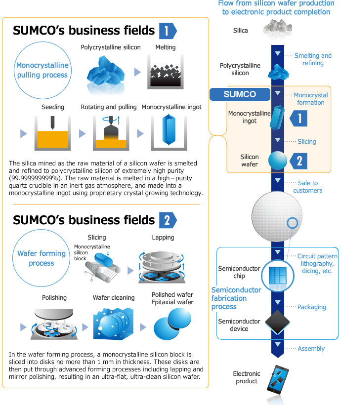
What Is Silicon Wafer Sumco Corporation


Comments
Post a Comment